

TSMC Boosts Arizona Investment to $265 Billion: A Strategic Shift for AI Semiconductors
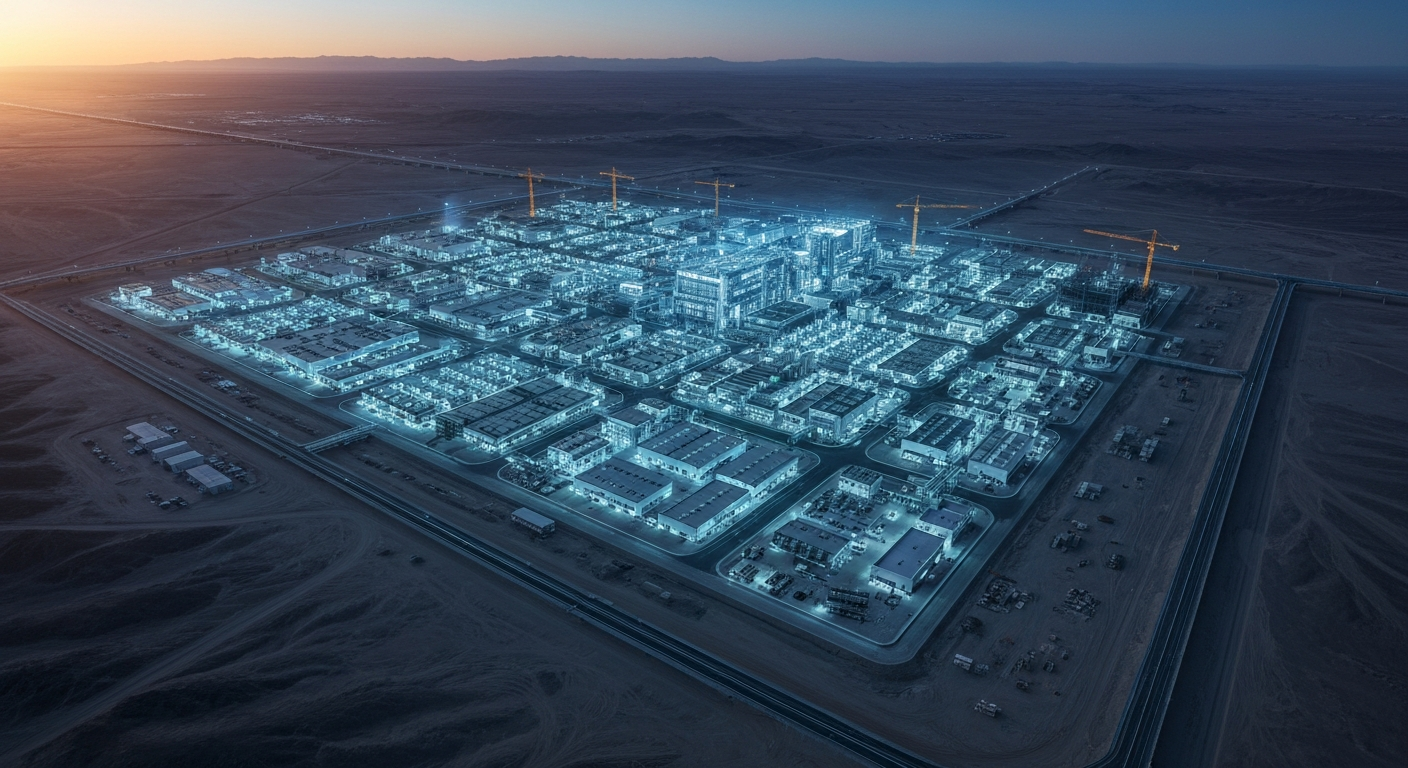
In a direct response to the explosive growth of the artificial intelligence (AI) chip market, which is on track to represent 30% of global semiconductor revenue by 2026, TSMC is placing a staggering $265 billion bet on Arizona. This commitment, boosted by an additional $100 billion and equivalent to roughly 397.5 trillion Korean Won, will fund an unprecedented build-out of 10 new semiconductor factories, two advanced packaging facilities, and an R&D center. This is not merely an expansion; it’s a fundamental move designed to meet long-term AI semiconductor demand and reshape the global supply chain.
This move is far more than a simple capacity increase; it’s a calculated response to immense pressure from key clients. Tech giants like NVIDIA, AMD, Apple, and Qualcomm are clamoring for more U.S.-based advanced manufacturing, specifically for chips built on 3nm technology and beyond. By building in Arizona, TSMC directly answers that call, cementing its indispensable role in the AI era. Sweetening the deal is the U.S. CHIPS and Science Act, which provides a crucial $11.6 billion in grants and loans to offset the high costs of overseas construction. With the global AI chip market projected to soar from $107.01 billion in 2026 to $592.61 billion by 2033, TSMC is positioning itself to dominate this lucrative future.
A core component of this strategy lies in the new advanced packaging facilities. For the intense computational demands of AI and high-performance computing (HPC), advanced packaging is non-negotiable. It allows multiple chiplets to act as a single, powerful system, slashing bottlenecks, boosting memory bandwidth, and improving power efficiency—all critical for scaling AI sustainably. Given that a staggering 98% of this advanced packaging currently happens in Asia, TSMC’s Arizona facilities represent a seismic shift for U.S. supply chain resilience and national security. This move unequivocally turns up the heat on competitors like Intel and Samsung, forcing them to accelerate their own U.S.-based advanced manufacturing and packaging roadmaps. TSMC is not just defending its foundry leadership; it’s accelerating the entire trend of supply chain regionalization.
This massive undertaking is not without significant hurdles. A critical shortage of skilled labor has already forced TSMC to dispatch roughly 3,000 engineers from Taiwan to Arizona. The desert location also raises legitimate concerns about water usage, though the company plans to mitigate this with advanced wastewater recycling systems targeting over 80% reuse. Beyond that, simple physical constraints like the availability of construction workers and infrastructure pose ongoing challenges. Despite these obstacles, early results are promising. The project’s first fab began high-volume production on its N4 process in the fourth quarter of 2024, impressively achieving yields on par with its leading-edge fabs in Taiwan. This initial success provides a crucial vote of confidence for the ambitious expansion ahead.
For investors, the trajectory of TSMC’s Arizona project, along with sustained U.S. government backing, is now a key focal point. The explosive AI semiconductor market provides a powerful tailwind for TSMC’s long-term growth, but the risks of rising costs and persistent labor shortages cannot be ignored and require masterful management. This isn’t just about one company’s growth; it’s a landmark event in the creation of a new, U.S.-centric global semiconductor ecosystem. Competitors must now urgently re-evaluate their own strategies in advanced packaging and R&D or risk being left behind. In the end, the true victors of the AI era will be defined not just by their ability to design chips, but by their mastery in building and managing these incredibly complex global supply chains.
References & Sources
